The FPGA Development Board
To start with, the Altera's Cyclone II FPGA Starter Development Board was obtained. Apart from a medium sized FPGA, the board has various types of memory (SRAM, SDRAM, Flash), physical IO interfaces (RS232, VGA, SD memory card, sound), switches and LEDs. By means of an USB connection, the board can be connected with a PC; over the USB connection a JTAG link between the Board and the PC is established to download FPGA configuration files to the Board. The JTAG link can also be used for communication between a program running in the FPGA and a program running on the PC.
The Development Board is part of a kit, which includes development software and program examples as well. To program the FPGA, the free Web edition of Altera's Quartus development system is used. This environment supports both VHDL and Verilog.
As a first somewhat larger experiment a rebuild, called X16, of the Honeywell 316/516 minicomputer was made. For this experiment, only the FPGA, part of the SRAM and some of the switches and LEDs are used. The objective of this effort was the make a replica of the 316/516 with a memory of 16k words, with a real time clock (RTC) and supporting a console TTY (TTY), a papertape reader (PTR) and puncher (PTP). Such a configuration would fit with the available standard papertape software (Assembler, Basic, Linker, Fortran, etc.).
The second version of X16 is supporting addressing up to 32 K words (and the Extended Mode option is added). At the same time some bugs are removed and some additional features are added (e.g. console logging).
The third version of X16 supports a faster papertape reader of 100 cps.
The remaining part of this page shows the design used for building the replica as well as some of the results.
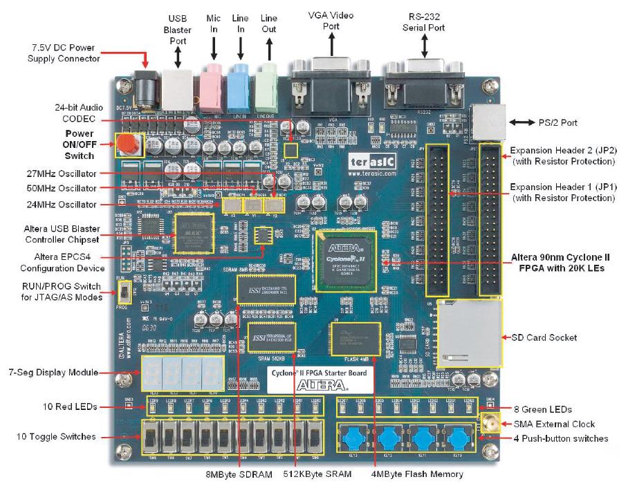
Cyclone II Starter Board
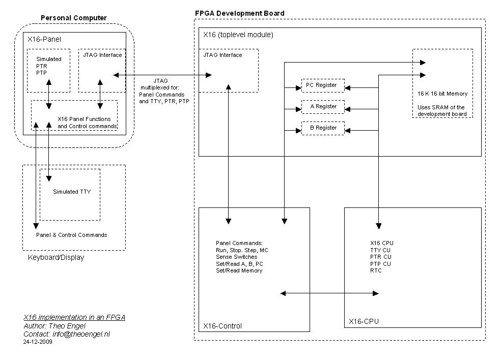
X16 block diagram
The X16 FPGA Design
The block diagram shows that at top level, the design is split in two main parts:
- Development Board part: CPU, Peripheral Control Units, Main Memory
- Personal Computer part: Panel Functions (Run, Stop, Step, etc.), Peripherals (TTY, PTR, PTP)
The CPU and the peripheral Control Units are implemented into the FPGA, while part of the SRAM chip on the Development Board is used for the main memory. For the peripherals itself, it was chosen to simulate them on the PC. Also all the computer panel functions are simulated on the PC. In order to get information from the simulated peripherals and panel to the CPU and CU's in the FPGA (and the other way around), the JTAG interface is used as a communication link. The JTAG link is multiplexed for the TTY input and output, the PTR and the PTP and for the Panel functions. Small information packets are exchanged to start, stop or single step the CPU, to set the Sense Switches and to set or read memory locations. These information packets also exchange the peripheral data bytes.
All Panel, peripheral and JTAG communication functions are concentrated in the PC-program X16Panel-xx.pl, which is written in Perl (ActiveState Perl is being used). For the JTAG-USB interface, use is made of the library/driver of Future Technology Devices International Ltd. (ftd2xx.dll, to be loaded in the directory where X16Panel-xx.pl is stored). The Panel program and driver are tested and used at this moment with Windows XP. The control commands that are supported by the Panel program are listed below.
The Development Board / FPGA part of the design is split over five files, written in Verilog:
- X16_xx.v (Top level, integrating the CPU, Memory, Control and Registers)
- X16_Cpu_xx.v (Cpu, Rtc, Peripheral control units)
- X16_Control_xx.v (Panel functions and communication with the PC)
- USB_JTAG.v (Altera distributed module for the JTAG interface)
- CLK_LOCK.v (Altera distributed module for the JTAG clock)
The Verilog X16 files can be found in the X16 directory. The USB_JTAG and CLK_LOCK files are Altera/Board specific, and are distributed as part of the Cyclone II development kit. In order to synthesize the design into a workable FPGA configuration file for the Development Board, also a pin declaration file must be supplied. This file binds the FPGA pins to the used interface signals (defined in X16_xx.v) and is also FPGA/Board specific.
The X16 CPU implements the standard instruction set. To simplify debugging however, the following "features" are added:
- each non-standard or not-existing instruction results in an error state and stops the CPU;
- a Breakpoint Register (BP) is added: when the CPU is running and the content of the Program Counter equals the content of the Breakpoint Register, the CPU stops (the initial value of BP is 0).
In addition, the X16Panel program supports a Trace command. With this command multiple Steps are executed, while after each Step the state of the CPU is displayed.
Each instruction is executed in multiple clock cycles. Generic instructions take 4 cycles. Simple memory reference instructions (JMP, ADD, STA, ...) with direct addressing take 4 cycles as well, while the more complex ones (IRS, CAS, ...) take 5 or 6 cycles. Each level of indirect addressing or indexing uses an additional cycle. The clock is derived from one of the crystal clocks available on the Development Board (50MHz, 27MHz and 24MHz). The design runs stable with either the 24MHz or 27MHz clock. So the shortest instruction time (the one of a Generic) is about 160 nsec, which is about 6 times faster compared with the execution time of a Generic on the DDP516.
When programming the logic for X16, the biggest hurdle to take was to understand that in an FPGA all operations in principle execute in parallel, while on a computer operations execute in sequence. On a computer special arrangements must be made to get parallelism e.g. by making something like multitasking. With an FPGA special arrangements must be made to get things executing in sequence e.g. by using state machines. The implementation of the CPU and the peripheral Control Units are based on such state machines, driven by the clock.
The whole design takes about 10% of the logical resources of the FPGA (which is a Cyclone II EP2C20F484C7 with 20k Logical Elements), while the design is straightforward without optimization (e.g. each operation where an adder is used has its own adder; not a single ALU to be shared for these operations is implemented). There is of course optimization applied by the synthesis tools at gate level. Version 03, with the faster papertape reader, uses additional logical resources; this design takes 11%.
The current version of X16 is version 04 (in the X16-04 directory )
- options: 32K 16bit words, RTC, Extended Mode
- supported peripherals: TTY, PTR and PTP
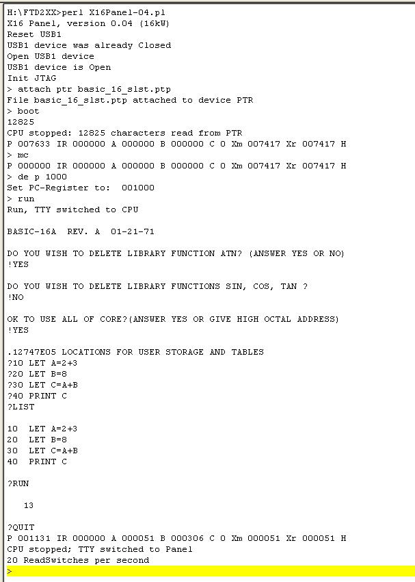
Basic booted and running on X16 controlled by X16Panel
The X16 Panel Control commands
The Panel program on the PC is started in a command line window with the command:
c:perl X16Panel-xx.pl.
Because most Panel commands are meant to interact with the programmed FPGA, the FPGA configuration file must be loaded into the FPGA before the Panel program on the PC is started.
The following control commands are supported by the Panel program:
- examine|ex <register> (show register content)- examine|ex m <address> (interactively shows content of <address>, <address>+1, .. until s is replied)
- deposit|de <register> [<16 bit value>] (if no content, content is requested until s is replied)
- deposit|de m <address> [<16 bit value>] (if no content, content is requested until s is replied)
- mc (master clear; reset the computer to its initial state)
- step (execute a single instruction)
- run (execute program, starting with the instruction set in the PC)
- stop|CntrE (stop program execution)
- state (request-display state of the cpu in the fpga)
- trace [n|>] (executes a single or n instructions showing state (> executes until CntrE)
- ss (sets/resets one or more sense switches)
- s? (show the sense switches setting)
- ldhex|ldh [s] <fn>.hex (load program into memory from a file (format: absolute hexadecimal))
- log [on|off] |
- attach|att ptr|ptp <file> (attach a file on disk to either the papertape reader (PTR) or puncher (PTP))
- detach|det ptr|ptp (the attached file will be detached from the device and the device is closed)
- reset ptr|ptp|mem (resets the PTR or PTP, or sets the memory to zero)
- boot (boot from the papertape reader (PTR must be attached to a file with proper papertape format)
- mode [hex|h] | [oct|o] (set console to either hex or octal; no argument, shows mode (default=octal))
- exit (disconnect from FPGA and the control program exits; reconnection later is possible by starting X16Panel again)
| means logical OR.
[..] means OPTIONAL argument.
<address> is hex value of 0..3FFF, or octal value 0..37777.
<register> is PC|P,A,B,X,BP (X=read only: the X=Register can be set by changing memory location 0).
When the TTY is used by the CPU, the key combination CntrE stops the execution of the CPU (like the stop command). BP is Breakpoint Register. At the end of the execution of an instruction, BP is compared with PC: the address of the next instruction to execute. In case BP and PC are equal, the CPU is stopped.
When the CPU stops execution (after Run or Step) the state of the CPU is displayed.
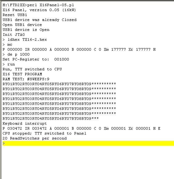
X16 running the test program TX16-2
X16 Testing
Unfortunately there are no original Honeywell 316/516 test programs available, at least I am not aware of those. So testing has to be done with own prepared test programs. During the development of the FPGA Verilog program, many small tests were required to check the operation of each instruction, the addressing mechanism, etc.
To simplify the generation of these small tests, a DAP16 compatible (from source language point of view) assembler was made, which produces hexadecimal output of absolute code that can easily be loaded into the SRAM of the Development Board (the ldhex command of X16Panel supports the loading of programs in that format). The assembler supports only a subset of the pseudo operations, and the output of the assembler cannot be linked. The assembler (X16Asm-xx.pl) is written in Perl and available in the X16 directory.
Also a test program (TX16-x), which checks most of the properties of the CPU, is available in this directory. The test program does not perform an in depth analysis of each instruction, but all instructions and features of the FPGA loaded computer are quickly checked by a single program, including the RTC, interrupt mechanism, all addressing modes, memory and TTY in and output.
The operation of MTK16, as presented elsewhere on this web site, is used as a test as well. The demo is linked and punched as a selfloading tape and loaded in X16 on the FPGA.
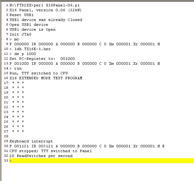
X16 running the Extended Mode test program TX16E-1
Demo: DAP16 assembly, load and execution of a small program
The execution of some other standard H316/516 software on X16-02 is presented on hello-world. The console interaction of this example is intermingled with comments to explain what is happening.
X16-02 supports the Extended Mode option, and with that is able to address 32 K words. LDR-APM, which is used in this demo, is running in the Extended Mode and looks to be OK. In addition to the test program TX16-x, an additional test program TX16E-x is added, which checks the various aspects of Extended Mode. Both TX16-x and TX16E-x are meant to check all properties of the CPU and their successful operation provides a minimum condition for a valid CPU implementation.
Demo: Fortran IV program compilation, load and execution
In the same way as the DAP16 assembly above, a Fortran compilation, load and execution is performed to check the validity of the X16 implementation. As Fortran test program, the Mandelbrot example of Philipp Hachtmann is taken. Also in this case the console interaction of the demo is intermingled with comments to explain what is happening.
The text of the demo is long because all details of all steps of the compile, load and execution process are presented. Also the time to complete this demo was long (1 hour+), mainly because the papertape reader is slow, and with that slow reader the long Fortran library has to be loaded. The speed of the papertape reader is about 20 chars/second during program execution. When booting, the PTR is much faster (about 900 chars/sec). During boot, the read characters from the PTR are just forwarded to the FPGA, because during boot the receiving process in the FPGA is fast enough to absorb the bytes. During program execution bytes are sent to the FPGA over the multiplexed JTAG connection only when there is a request from the FPGA. This handshaking slows down the reading speed of the PTR. Another mechanism is to be investigated to increase the speed of the PTR during program execution. However the demo executes as expected and all peripherals are used during the compilation over the multiplexed JTAG and operate well (except from the speed issue). So for the moment the system looks to be OK.
X16-02 performs well except the papertape reader slows down the system performance. Version 03 is an attempt to improve the papertape reader throughput.
The bottleneck is the throughput of the JTAG link. The JTAG is a 1Mhz link, and when used for booting a program, the throughput is about 1000 messages per second from the PC to the FPGA, which equals to about 700 Kbps (1000 * 9 chars * 8 bit). Nothing wrong with that. However when the JTAG link is, during program excution, used in handshaking mode, the throughput drops down to 20 messages/sec from the PC to the FPGA and 20 messages/sec from FPGA to PC (20 * (9 + 15) chars * 8 bit), which is about 4 Kbps. The difference is that the sending direction is changed after each message sent. Is that changing of the sending direction explaining that big difference ??
Anyhow, in order to improve the PTR throughput, special PTR packets in X16-03 are supported, which transfer 5 bytes at once to a buffer in the FPGA and from there, on request, one by one to the PTR control unit. When the buffer is exhausted, the request from the PTR control unit for a byte is forwarded to the PC, which replies again with a packet of 5 bytes. This indeed improves the throughput about five times. Loading time for the Fortarn IV example is reduced to 10 minutes.
X16-03 uses for booting a program the same PTR logic as used before. However when the PTR is used under program control, the faster PTR logic is used (the selection for which logic to use is made by the X16Panel program).
X16-03/X16-04 running Fortran IV
note: X16-03/X16-04 are running with X16Panel-09.pl and later.